← Alpine IVE-W530BT Wiring – The Car Audio Upgrade You Need! A complete guide to alpine car stereo wiring diagram 450W Mono Amplifier Using A5198 & A1941: Build Your Sound System! Best 13 diy amplifier circuit using c5198 and a1941 – artofit →
If you are searching about Capture Pads and Non-functional Pads in PCB Design: What Are They? you've visit to the right page. We have 25 Images about Capture Pads and Non-functional Pads in PCB Design: What Are They? like Should Non-Functional Pads be Removed or Kept in Vias of High-Speed PCB, Removing Non-Functional Pads and Routing Conductors - Summit Interconnect and also PCB Vias: An In-Depth Guide. Read more:
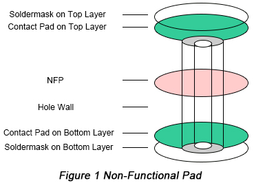
Capture Pads And Non-functional Pads In PCB Design: What Are They?
Capture Pads and Non-functional Pads in PCB Design: What Are They?
Use It Or Lose It? What Should You Do With Non-Functional Pads
1.jpg) www.allaboutcircuits.com
www.allaboutcircuits.com
Use It Or Lose It? What Should You Do with Non-Functional Pads ...
Lifted Pads On PCBs - Causes, Repairs, And Prevention - GlobalWellPCBA
 www.globalwellpcba.com
Lifted Pads on PCBs - Causes, Repairs, and Prevention - GlobalWellPCBA
Should Non-Functional Pads Be Removed Or Kept In Vias Of High-Speed PCB
 www.pcbcart.com
Should Non-Functional Pads be Removed or Kept in Vias of High-Speed PCB ...
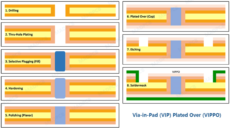
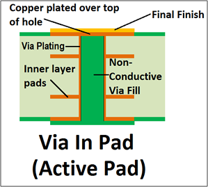
Understanding Via In Pad In PCB-types, Advantages, Process, Filling
 www.pcbaaa.com
Understanding via in pad in PCB-types, advantages, process, filling ...
Via In Pad Manufacturing Process | PCB Manufacturer | MADPCB
 madpcb.com
Via in Pad Manufacturing Process | PCB Manufacturer | MADPCB
PCB Pad – A Basic Guide For Beginners - Mainpcba One-stop PCB Assembly
 www.mainpcba.com
PCB pad – a basic guide for beginners - Mainpcba One-stop PCB Assembly ...
PCB Via In PAD - Pcbsfactory.com
 pcbsfactory.com
PCB Via in PAD - pcbsfactory.com
PCB Vias - Everything You Need To Know
 blog.epectec.com
PCB Vias - Everything You Need To Know
PCB Vias: An In-Depth Guide
 www.epiccolo.com
PCB Vias: An In-Depth Guide
The Complete Guide To PCB Pad :types, Size, Spacing, Repair And
 www.pcbaaa.com
The complete guide to PCB pad :types, size, spacing, repair and ...
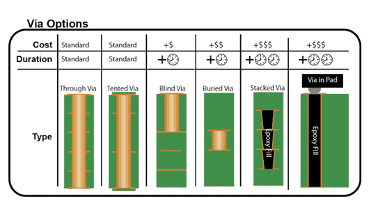
A Complete Guide To Vias In PCB Design - Electronics Post
 electronicspost.com
A Complete Guide to Vias in PCB Design - Electronics Post
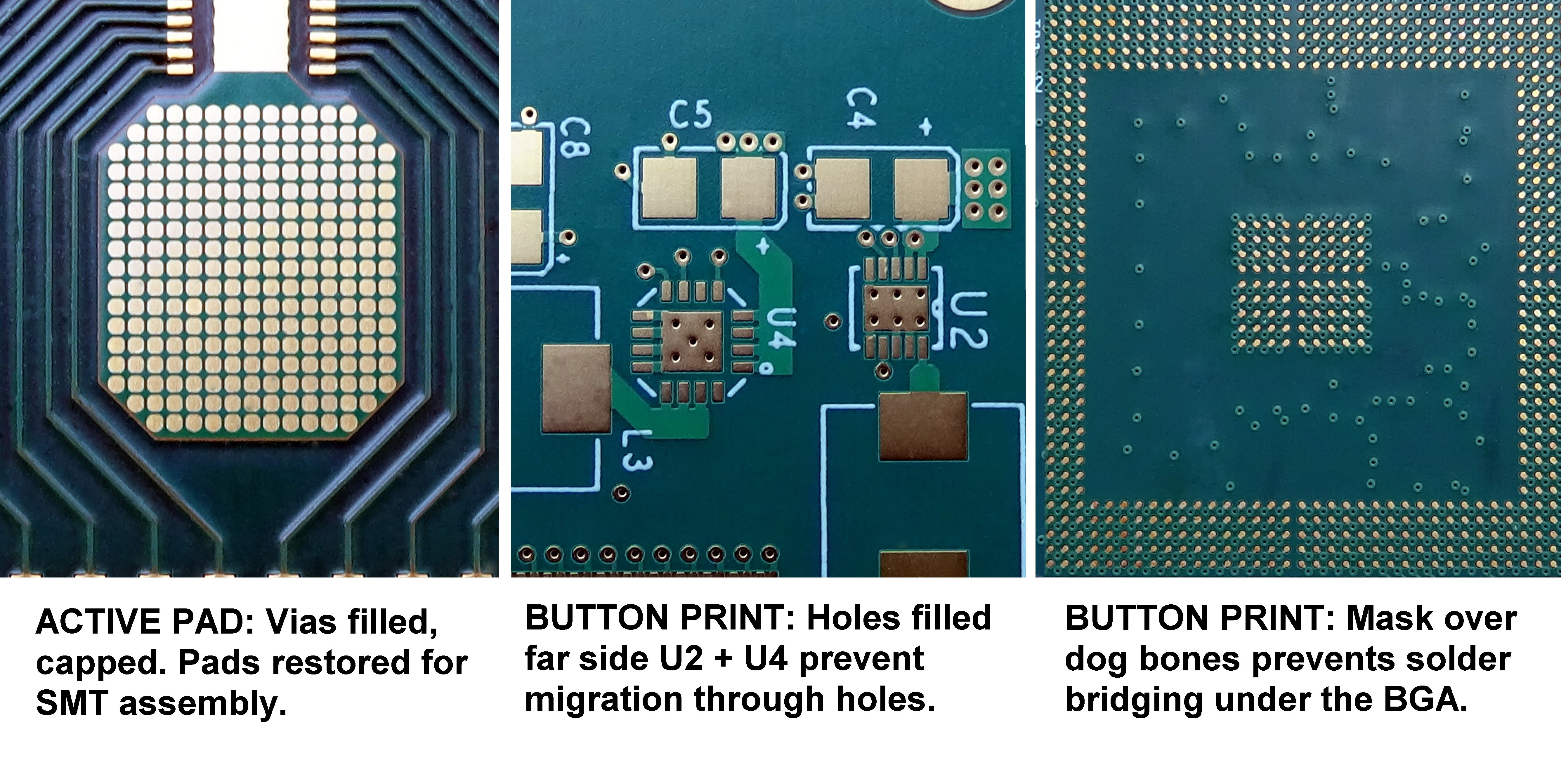
How Non-functional Pads Affect Your PCB Design | PCB Routing
 resources.altium.com
How Non-functional Pads Affect Your PCB Design | PCB Routing
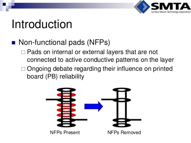
Non Functional-pads-should-they-stay-or-should-they-go
 www.slideshare.net
Non functional-pads-should-they-stay-or-should-they-go
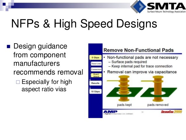
Non Functional-pads-should-they-stay-or-should-they-go
 www.slideshare.net
Non functional-pads-should-they-stay-or-should-they-go
What Is A Pad In PCB Design And Development | Sierra Circuits
 www.protoexpress.com
What is a Pad in PCB Design and Development | Sierra Circuits
How PCB Vias Interconnect Circuit Board Layers | Sierra Circuits
 www.protoexpress.com
How PCB Vias Interconnect Circuit Board Layers | Sierra Circuits
What Are Vias In PCBs? | PCB Prime
 pcbprime.com
What Are Vias in PCBs? | PCB Prime
Removing Non-Functional Pads And Routing Conductors - Summit Interconnect
 summitinterconnect.com
Removing Non-Functional Pads and Routing Conductors - Summit Interconnect
Do You Really Need Via-in-Pad?
 pcbtrace.com
Do You Really Need Via-in-Pad?
Using Via-in-Pad Technology: What You Need To Know, Design Guidelines
Using Via-in-Pad Technology: What You Need to Know, Design Guidelines ...
PCB Pads - MorePCB
 morepcb.com
PCB Pads - MorePCB
PCB Vias: An In-Depth Guide (2023)
 indodepo303.com
PCB Vias: An In-Depth Guide (2023)
What Is A PCB Via? A Complete Guide!
 www.elepcb.com
What is a PCB via? A complete guide!
PCB Vias: An In-Depth Guide
 www.epiccolo.com
PCB Vias: An In-Depth Guide
Understanding via in pad in pcb-types, advantages, process, filling .... Capture pads and non-functional pads in pcb design: what are they?. What is a pcb via? a complete guide!